TSMC Celebrates 30th North America Technology Symposium with Innovations Powering AI with Silicon Leadership
24 Abril 2024 - 2:30PM
Business Wire
TSMC (TWSE: 2330, NYSE: TSM) today unveiled its newest
semiconductor process, advanced packaging, and 3D IC technologies
for powering the next generation of AI innovations with silicon
leadership at the Company’s 2024 North America Technology
Symposium. TSMC debuted the TSMC A16TM technology, featuring
leading nanosheet transistors with innovative backside power rail
solution for production in 2026, bringing greatly improved logic
density and performance. TSMC also introduced its System-on-Wafer
(TSMC-SoW™) technology, an innovative solution to bring
revolutionary performance to the wafer level in addressing the
future AI requirements for hyperscaler datacenters.
This year marks the 30th anniversary of TSMC’s North America
Technology Symposium, and more than 2,000 attended the event,
growing from less than 100 attendees 30 years ago. The North
America Technology Symposium in Santa Clara, California kicks off
TSMC Technology Symposiums around the world in the coming months.
The symposium also features an “Innovation Zone,” designed to
highlight the technology achievements of our emerging start-up
customers.
“We are entering an AI-empowered world, where artificial
intelligence not only runs in data centers, but PCs, mobile
devices, automobiles, and even the Internet of Things,” said TSMC
CEO Dr. C.C. Wei. “At TSMC, we are offering our customers the most
comprehensive set of technologies to realize their visions for AI,
from the world’s most advanced silicon, to the broadest portfolio
of advanced packaging and 3D IC platforms, to specialty
technologies that integrate the digital world with the real
world.”
New technologies introduced at the symposium include:
TSMC A16TM Technology: With TSMC’s industry-leading N3E
technology now in production, and N2 on track for production in the
second half of 2025, TSMC debuted A16, the next technology on its
roadmap. A16 will combine TSMC’s Super Power Rail architecture with
its nanosheet transistors for planned production in 2026. It
improves logic density and performance by dedicating front-side
routing resources to signals, making A16 ideal for HPC products
with complex signal routes and dense power delivery networks.
Compared to TSMC’s N2P process, A16 will provide 8-10% speed
improvement at the same Vdd (positive power supply voltage), 15-20%
power reduction at the same speed, and up to 1.10X chip density
improvement for data center products.
TSMC NanoFlexTM Innovation for Nanosheet Transistors:
TSMC’s upcoming N2 technology will come with TSMC NanoFlex, the
company’s next breakthrough in design-technology co-optimization.
TSMC NanoFlex provides designers with flexibility in N2 standard
cells, the basic building blocks of chip design, with short cells
emphasizing small area and greater power efficiency, and tall cells
maximizing performance. Customers are able to optimize the
combination of short and tall cells within the same design block,
tuning their designs to reach the optimal power, performance, and
area tradeoffs for their application.
N4C Technology: Bringing TSMC’s advanced technology to a
broader range of of applications, TSMC announced N4C, an extension
of N4P technology with up to 8.5% die cost reduction and low
adoption effort, scheduled for volume production in 2025. N4C
offers area-efficient foundation IP and design rules that are fully
compatible with the widely-adopted N4P, with better yield from die
size reduction, providing a cost-effective option for value-tier
products to migrate to the next advanced technology node from
TSMC.
CoWoS®, SoIC, and System-on-Wafer (TSMC-SoW™ ): TSMC’s
Chip on Wafer on Substrate (CoWoS®) has been a key enabler for the
AI revolution by allowing customers to pack more processor cores
and high-bandwidth memory (HBM) stacks side by side on one
interposer. At the same time, our System on Integrated Chips (SoIC)
has established itself as the leading solution for 3D chip
stacking, and customers are increasingly pairing CoWoS with SoIC
and other components for the ultimate system-in-package (SiP)
integration.
With System-on-Wafer, TSMC is providing a revolutionary new
option to enable a large array of dies on a 300mm wafer, offering
more compute power while occupying far less data center space and
boosting performance per watt by orders of magnitude. TSMC’s first
SoW offering, a logic-only wafer based on Integrated Fan-Out (InFO)
technology, is already in production. A chip-on-wafer version
leveraging CoWoS technology is scheduled to be ready in 2027,
enabling integration of SoIC, HBM and other components to create a
powerful wafer-level system with computing power comparable to a
data center server rack, or even an entire server.
Silicon Photonics Integration: TSMC is developing Compact
Universal Photonic Engine (COUPE™ ) technology to support the
explosive growth in data transmission that comes with the AI boom.
COUPE uses SoIC-X chip stacking technology to stack an electrical
die on top of a photonic die, offering the lowest impedance at the
die-to-die interface and higher energy efficiency than conventional
stacking methods. TSMC plans to qualify COUPE for small form factor
pluggables in 2025, followed by integration into CoWoS packaging as
co-packaged optics (CPO) in 2026, bringing optical connections
directly into the package.
Automotive Advanced Packaging: After introducing the N3AE
“Auto Early” process in 2023, TSMC continues to serve our
automotive customers’ needs for greater computing power that meets
the safety and quality demands of the highway by integrating
advanced silicon with advanced packaging. TSMC is developing
InFO-oS and CoWoS-R solutions for applications such as advanced
driver assistance systems (ADAS), vehicle control, and vehicle
central computers, targeting AEC-Q100 Grade 2 qualification by
fourth quarter of 2025.
About TSMC
TSMC pioneered the pure-play foundry business model when it was
founded in 1987, and has been the world’s leading dedicated
semiconductor foundry ever since. The Company supports a thriving
ecosystem of global customers and partners with the industry’s
leading process technologies and portfolio of design enablement
solutions to unleash innovation for the global semiconductor
industry. With global operations spanning Asia, Europe, and North
America, TSMC serves as a committed corporate citizen around the
world.
TSMC deployed 288 distinct process technologies, and
manufactured 11,895 products for 528 customers in 2023 by providing
broadest range of advanced, specialty and advanced packaging
technology services. The Company is headquartered in Hsinchu,
Taiwan. For more information please visit https://www.tsmc.com.
View source
version on businesswire.com: https://www.businesswire.com/news/home/20240424036229/en/
TSMC Spokesperson: Wendell
Huang Senior Vice President and CFO Tel: 886-3-505-5901
Media Contacts: Nina Kao
Head of Public Relations Tel: 886-3-563-6688 ext.7125036 Mobile:
886-988-239-163 E-Mail: nina_kao@tsmc.com
Michael Kramer Public Relations Tel: 886-3-563-6688 ext. 7125031
Mobile: 886-988-931-352 E-Mail: pdkramer@tsmc.com
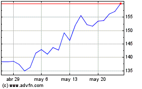
Taiwan Semiconductor Man... (NYSE:TSM)
Gráfica de Acción Histórica
De Abr 2024 a May 2024

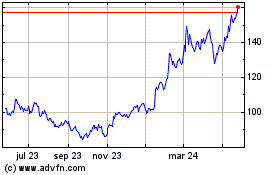
Taiwan Semiconductor Man... (NYSE:TSM)
Gráfica de Acción Histórica
De May 2023 a May 2024
